
At CoderDojo Oradea Space Robotics, we believe that the most valuable data comes not just from successful flights, but from understanding exactly why things didn't go as planned. This year, our CanSat 2026 Nationals entry did not place in the top three. The board never completed a clean power-on in flight configuration, and neither of our two mission objectives was exercised in the air.
This post is the full engineering post-mortem. It documents what we set out to build, the decisions we made along the way, what failed and why, and the specific design changes that will shape our next iteration. It is written primarily for the engineering community and for the CDOSR students who will inherit this project, but we believe it has value for any team operating under the kind of compounding constraints, schedule, supply chain, internal volume, power budget, that define competitive CanSat work.
Our team of six students, Alin Lupău, Antonio Laza, Mark Trefi, Cristina Andor, Erik Bunea, and Matei Ciuca, spent the better part of an academic year on this payload. The flight didn't happen this time. The learning did.
The Mission Architecture
Our goal was a dual-objective payload housed inside a custom Sears-Haack (teardrop) fuselage, optimised for low-drag descent and tight internal packaging.
Primary mission: continuous telemetry of temperature, pressure, and humidity, transmitted via GSM/GPRS at a minimum rate of 1 Hz throughout the descent. The atmospheric profile would be reconstructed on the ground station from the timestamped packets, with cellular telemetry chosen over an RF link both for range (no line-of-sight requirement) and for the ability to recover data even from an off-nominal landing site.
Secondary mission: an autonomous guided descent under a steered 9-cell ram-air parafoil, supplemented by brushless thrust for active glide management. A flight controller running on the main ESP32-S3 would execute a PID control loop fusing GPS position and IMU attitude, with the objective of landing within 100 m of a pre-programmed waypoint and a heading error of less than 20° RMS.
The combination is non-trivial. Guided parafoils have flown on CanSats before, but pairing one with active brushless propulsion and cellular telemetry inside a fuselage designed for aerodynamic efficiency rather than electronics integration pushed every subsystem toward its boundary at the same time.
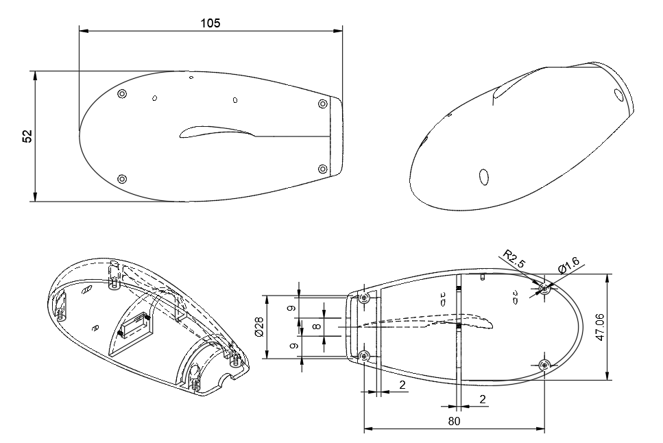 The custom Sears-Haack fuselage. The teardrop profile minimises drag for the descent phase but leaves no margin for traditional multi-board electronics stacks.
Subsystem Breakdown
The integrated electronics platform consolidated the following onto a single PCB:
- Compute: ESP32-S3-WROOM-1 module, selected for its dual-core architecture, native USB, and adequate RAM for the PID loop and telemetry buffering.
- Atmospheric sensing: Bosch BME688 for temperature, pressure, humidity, and gas resistance.
- Inertial sensing: InvenSense MPU-9250 (accel + gyro + magnetometer) for attitude estimation feeding the parafoil control loop.
- Positioning: u-blox NEO-M9N GNSS module, multi-constellation, selected for fast cold-start performance and compact footprint.
- Power management: Texas Instruments BQ25887 single-cell Li-ion charger with integrated MPPT pin, and an LTC2943 fuel gauge for state-of-charge reporting in telemetry.
- Telemetry: Quectel M66 GSM/GPRS modem, with on-board SIM socket and the required RF front-end matching.
- Actuation: brushless ESC driving a small pusher motor for active glide, plus two micro servos for parafoil line steering.
Consolidating all of this onto a single board was the central architectural choice. In previous seasons we flew multi-board stacks connected by ribbon cables and pin-header connectors, and we had repeatedly observed that the connectors themselves were a recurring failure mode, both during ground handling and after vibration loads on descent. The Sears-Haack internal volume made a stack physically impossible regardless: there was simply no cylindrical region inside the fuselage where conventionally shaped boards would fit.
The integrated single-board approach solved both problems. It also created a new one, which is the subject of the rest of this post.
The Engineering Challenge: When Theory Meets Logistics
The target design was a 6-layer PCB. The stackup was chosen specifically for the combination of high-current motor switching, sensitive RF, and mixed-signal sensor returns on a single board. The two inner planes were dedicated to a continuous ground pour and a clean VBUS rail, with the four outer signal layers carrying routing partitioned between the digital, analog, and RF domains.
This is not a luxury choice for this kind of payload. On a board where:
- a brushless ESC draws transient currents in the tens of amps through traces only millimetres from the GPS antenna feed,
- a cellular modem at 2 W peak transmit power sits within centimetres of a 9-axis IMU,
- and the system clock for the PID loop must remain stable across all of this,
the isolation between domains is not decorative. It is what makes the board work at all.
We submitted the 6-layer design to fabrication on schedule. Then we learned what every hardware team eventually learns: published fab lead times are not commitments.
The delay was not catastrophic in isolation, a couple of weeks, but it was enough to push delivery past the date by which we needed populated boards in hand to begin bring-up, debug, software integration, and at least one round of rework if necessary. With zero margin for any of that, we faced a binary decision: wait for the 6-layer boards and miss the competition, or pivot.
The Pivot: A 4-Layer Contingency
We chose to pivot. We had a 4-layer board on hand, derived from our test hardware earlier in the design cycle, sharing most of the schematic but with a reduced stackup that we had originally used only for prototyping the firmware against real sensor silicon. We adapted the test board to flight-configuration silkscreen, populated it with flight-grade components, and prepared for bring-up.
This was a decision made under time pressure, with known risks, by a team that understood the implications. We want to be precise about that, because the more common framing, "supply chain issues forced our hand", softens what is actually a planning failure on our part. We committed to a 6-layer design without building a lead-time buffer into our schedule that matched the fabrication risk we were taking. The fab being late was the proximate cause. Treating fabrication lead time as an external variable rather than a planning input was the root cause.
What the 4-Layer Cost Us
The reduced stackup forced three compounding compromises, each of which we documented at the time and accepted as a known risk:
Power distribution. The dedicated VBUS plane disappeared. Power to the high-current consumers, the ESC, the GSM modem during transmit bursts, the servos — was instead delivered through routed traces. The VBAT input from the battery, which on the 6-layer design entered through a continuous plane region with extensive copper area, was reduced on the 4-layer to routed traces dimensioned according to standard IPC-2152 guidelines for the steady-state operating current. The brushless ESC alone can pull peak currents several times higher than its steady-state rating during commutation events, and the 7.4 V 30C flight pack is rated to deliver tens of amps on demand. Without a plane region to spread that current over significant copper area, the traces became the single most thermally constrained element on the entire board.
Grounding. The continuous ground plane became a set of partial pours stitched together by vias and routing. For digital circuits running at moderate clock rates this is usually survivable. For our combination, an RF front-end whose return currents need a low-impedance path back to the modem, an IMU whose noise floor sets the limit on attitude estimation accuracy, and switching power circuitry whose ground bounce can couple into both, it was the most consequential of the three compromises. Return current paths were no longer obvious to predict and the layout could not guarantee that they would not loop through sensitive sections.
Isolation. With one fewer signal layer to work with, the routing of high-current rails moved into the same physical regions as the RF and IMU domains. Manual via stitching attempted to preserve isolation but could not replicate what a dedicated plane provides. Coupling between the motor switching domain and the inertial sensors was something we expected to see in bring-up; we hoped it would be tolerable rather than disqualifying.\
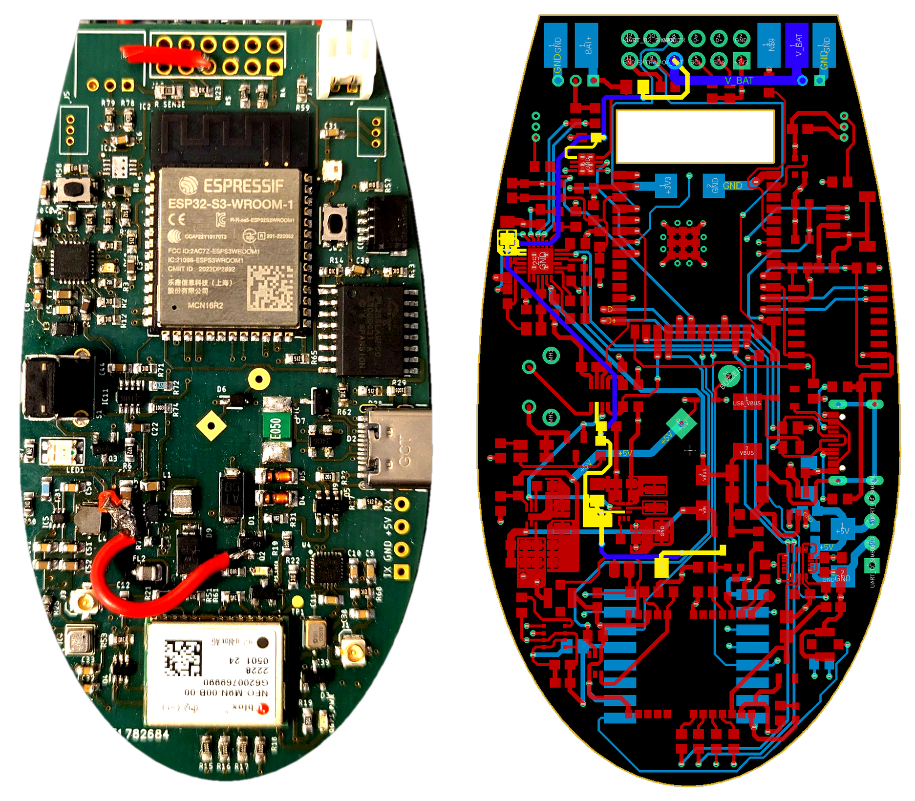 The 4-layer board layout that flew. The highlighted yellow and blue traces show the manually routed power rails that would have been a continuous VBUS plane on the 6-layer design. The fragmented ground pour is visible on the lower portion.
Each of these compromises was, on its own, survivable. The board could have worked. We have run all three of these conditions individually on test hardware in the past and seen the system function. What we underestimated was the interaction between them.
The Outcome
The board entered final assembly the week before the competition. Bring-up proceeded as far as basic peripheral enumeration: the ESP32-S3 booted, the GNSS module acquired a satellite fix, the BME688 reported sensible atmospheric values, and the GSM modem completed network registration. From a functional-block perspective, the system appeared viable.
The failure was sudden and unambiguous. Upon connecting the 7.4 V, 30C lithium-polymer flight pack and powering the system into full mission configuration, the VBAT input traces drew approximately 27 A and burned. The board was unrecoverable.
A 30C-rated 7.4 V pack is capable of delivering instantaneous currents well into the tens of amps, that is what the rating means and why a pack of this class is chosen for systems with brushless propulsion. The pack was behaving exactly as specified. The traces were not dimensioned to survive that current. On the original 6-layer design, VBAT entered the board through a dedicated plane region with adequate copper area and via fan-out to handle this class of inrush event. On the 4-layer, VBAT entered through routed traces dimensioned for steady-state operating current with conventional margins. Those margins were not sufficient for the actual transient envelope the system would see on first power-up under load.
This is, in retrospect, the cleanest possible illustration of the central thesis of this post-mortem. The trade-off we accepted when we pivoted from the 6-layer to the 4-layer was not abstract. It was specifically that we were giving up the copper area that would have carried this current. The board failed at the exact point where the compromise was made.
The competition flight did not proceed. We did not place in the top three.
Why This Matters
In the world of embedded systems and aerospace, "failure" is just data, but only if you actually extract the data. The temptation after a result like this is to file it under "supply chain bad luck" and move on. That would waste the most expensive learning experience the team had all year.
Here is what we actually learned. Not the obvious lessons, those were predictable from the setup, but the ones that will change how we plan and design next season.
Layer Count Is Not a Cost Metric
The cheapest framing of PCB layer count is as a per-square-inch cost line in the BOM. That framing is wrong in the same way that "RAM is just a cost line" is wrong, it is true at the level of accounting and false at the level of engineering. Layer count is a constraint on what the board can physically do. A 4-layer board cannot give you a continuous power plane and a continuous ground plane and signal routing for a board this dense. The geometry forbids it. When you reduce layer count, you are not saving money; you are choosing which electrical guarantees you are willing to lose. Future trade studies need to treat layer count as a primary design variable, not a cost-optimisation variable.
Single-Board Consolidation Cuts Both Ways
The motivation for consolidating onto a single board was sound: every inter-board connector is a failure mode, and we had been burned by connectors before. What we underestimated is the symmetric cost. On a multi-board stack, a layout compromise in the power section is contained to the power board. On a single integrated board, the same compromise touches every subsystem on the same copper. There is no longer a "telemetry board" you can isolate, swap, or substitute. The connector failure mode was real, but it had a property we lost when we eliminated it: it was localised.
Test Hardware Is Not a Flight Contingency
The deepest lesson of this season is the one we did not articulate explicitly during design review, and which therefore shaped our decisions silently. We had a 4-layer test board sitting on the bench. The unstated assumption, never stated, never challenged, never written down, was that if anything went wrong with the 6-layer, we could "fall back to the test board." This assumption shaped our schedule choices months before the pivot. We accepted a tighter fabrication window than we should have, because there was always the safety net.
The test board was never designed to be a flight contingency. It was designed to be a firmware development platform. The two are not the same thing, and treating the first as a backup for the second is a category error. In future design reviews, "what is our contingency if the primary board does not arrive in time?" will be an explicit question with an explicit answer, and the answer "we'll fly the test board" will be a flag for further discussion, not a resolution.
Schedule Risk and Design Risk Compound Nonlinearly
A two-week fabrication delay on a robust design is an inconvenience. The same delay on a design whose only fallback is a known-marginal alternative becomes a forced compromise on the highest-risk subsystem in the system. The mathematics of schedule risk and design risk are multiplicative, not additive: tight schedule × marginal fallback = guaranteed compromise on the most important board. Either factor on its own is manageable. Together, they remove the team's ability to make engineering decisions on engineering grounds.
What the Next Board Looks Like
The Sears-Haack aerodynamic profile validated in simulation and in mechanical fit. The single-board architecture remains the right direction. The specific changes for the next iteration are:
Stackup first. The next design begins with a power-and-ground stackup specification derived from the worst-case current demands of the mission profile, not from a target layer count. Layer count is the output of that analysis, not the input.
Hard go/no-go date for fabrication ordering. A specific calendar date will be set at the start of the design cycle, derived backward from the competition date with explicit buffers for fab lead time, assembly, bring-up, debug, and one full round of rework. Submitting after that date will require an explicit team decision and a documented plan for what we are giving up.
Separate flight hardware from development hardware. The next test board will be designed explicitly as a development board, different form factor, full debug connectors, no expectation of flight readiness. This removes the silent assumption that test hardware is a flight contingency.
Power budget validation as a gating milestone. Before final layout, we will calculate the worst-case current draw on every power rail in the system — explicitly including the maximum sustained and transient delivery capability of the chosen battery pack, not just the steady-state demand of the loads. VBAT traces and plane regions will be dimensioned to survive the pack's deliverable current envelope, with thermal headroom, and this calculation will be a documented checklist item in design review.
Vibration testing on populated hardware before flight. We will build a small shaker fixture and run the populated board through representative vibration profiles before the competition, both to catch mechanical failures and to characterise the IMU's noise floor in a more realistic environment.
Acknowledgments
This work would not have been possible without our six students, who spent months on a design that didn't get the flight it deserved and who showed up to the post-competition debrief ready to talk about the next one. The technical and personal maturity to do that is uncommon at any age. They are: Alin Lupău, Antonio Laza, Mark Trefi, Cristina Andor, Erik Bunea, and Matei Ciuca.
We thank Spark Communication for their sponsorship of our robotics program and for their patience with a season whose visible outcome did not match its underlying progress.
We thank the organisers of CanSat 2026 Nationals for the competition itself, and the other teams for raising the bar that we will be aiming for next year.
An Open Question for the Engineering Community
For teams running brushless propulsion and an RF telemetry front-end on a single compact board: how are you handling switching noise isolation when a dedicated ground plane is not available? We are genuinely interested in what has worked for others. Comments on this post are welcome.